Research Review: FER: A Benchmark for the Roofline Analysis of FPGA Based HPC Accelerators
- DSS Modeling

- Oct 25, 2025
- 8 min read
Background: The "Research Review" series is a grouping of articles that review scientific publications on the topics of financial modeling, foundation mathematics, and parallel computing. It is meant to enrich the community with technical knowledge and provide clarity on topics that can create distrust in the markets
Paper being review: E. Calore and S. F. Schifano, "FER: A Benchmark for the Roofline Analysis of FPGA Based HPC Accelerators," in IEEE Access, vol. 10, pp. 94220-94234, 2022, doi: 10.1109/ACCESS.2022.3203566.
Introduction
To optimize a Field-Programmable Gate Array (FPGA) design, an Agent requires a formal mathematical model—either empirical (based on measurements) or analytical (based on first principles)—to guide the optimization. This model must allow the Agent to infer optimal actions, such as minimizing memory block transfers between storage and the processing pipeline. The paper reviewed addresses this by proposing the authors' FPGA Empirical Roofline (FER) benchmarking tool as a modeling strategy to evaluate FPGA designs and generate chain-of-logic decision trees for design optimization.
This research article, titled "FER: A Benchmark for the Roofline Analysis of FPGA Based HPC Accelerators", focuses on providing a critical tool for performance evaluation of Field-Programmable Gate Arrays (FPGAs) utilized as accelerators in High Performance Computing (HPC) environments.
Given the increasing adoption of FPGAs in HPC systems, developers and system architects require reliable methods to estimate achievable performance. To satisfy these requirements, the authors have developed FER (FPGA Empirical Roofline). FER is a benchmarking tool engineered to empirically measure the computing performance of FPGA based accelerators and the bandwidths of their on-chip and off-chip memories. The resulting FER measurements enable the construction of Roofline plots for FPGAs, which facilitates direct performance comparisons with other processor types, such as CPUs and GPUs, while simultaneously providing an estimate of the maximum performance upper-bounds that applications can potentially achieve on a specific target device.
The document further describes the theoretical model that underpins FER, provides comprehensive details of its implementation (which uses a directives annotated C/HLS kernel), and presents experimental results measured on various Xilinx Alveo accelerator cards. This tool is distinguished as the first, developed using a pragma directives based high-level programming paradigm, that benchmarks FPGA accelerators within the Roofline Model framework while specifically accounting for on-chip memories
Mathematical Foundations
The core mathematical foundation discussed in the paper is the Roofline Model, which is a visual performance model used to provide performance upper bounds for compute kernels on a target architecture. The most basic Roofline plot illustrates the maximum computational performance (e.g., FLOP/s) achievable by an application as a function of its arithmetic intensity (I=O/D). Arithmetic intensity (I) is defined as the ratio of the number of operations performed (O, e.g., FLOPs) to the amount of data exchanged with memory (D, e.g., Bytes).
Each computing architecture is characterized by a specific machine balance (Mb=C/B), where C is the peak compute performance (e.g., maximum theoretical FLOP/s) and B is the peak memory bandwidth (e.g., maximum theoretical Byte/s). The performance an application reaches is limited either by the peak compute performance (if I is greater than Mb) or by the peak memory bandwidth (if I is lower than Mb). This document, which presents the FPGA Empirical Roofline (FER) benchmarking tool, relies on a theoretical model to link empirical performance results to the underlying hardware resources of FPGAs.
The theoretical model for FPGAs extends the standard Roofline concept by relating the peak computational performance (C) to the available hardware resources (Rkav) and the resources required by a specific operation (Rkop), along with the operating frequency (f). An initial formula for theoretical peak compute performance C for a given operation op is C=fop×(RopRav), assuming a single type of resource and ideal operation per clock cycle.
This is then extended to account for different types of resources (k) available on the FPGA (like LUTs, FFs, DSPs, etc.) using the minimum resource ratio, where C=fop×mink(RkopRkav). For a more accurate and realistic performance estimation, especially when large fractions of resources are used, the model is refined to incorporate the actual implemented design clock frequency (fimp) and resource utilization factors (uRk), leading to the equation: C=fimp×mink(RkopRkav×uRk). Similarly, the peak memory bandwidth (B) for on-chip memories (like BRAM/URAM) is modeled by Bram=fimp×Wram×RRAMav×uRRAM. The bandwidth for off-chip memories (DDR or HBM) accounts for both the kernel frequency (fimp) and the external memory frequency (fext), taking the minimum bandwidth of the on-chip and off-chip interfaces.
In practice, FER adopts an elementary RTL core from the IP library, such as a floating-point addition or multiplication, as the Processing Element (PE) for its calculations, which is not tied to any specific algorithm but is commonly used by generic HPC kernels.


Experimental Setup
The FPGA Empirical Roofline (FER) benchmark is configurable to run in two primary modes, which dictate how data is managed and where the memory bandwidth is measured. These two modes, which are essentially two different kernels, provide the same interface but are used alternatively to measure different memory hierarchies:
Dataflow Mode (dataflow)
Datalocal Mode (datalocal)
Dataflow Mode
The dataflow mode is designed to measure peak performance values achievable when data is kept in off-chip memories (e.g., on-board DDR or High Bandwidth Memory (HBM) banks) .
Kernel Organization: In this mode, the computation is structured as a task-level pipeline defined by the High-Level Synthesis (HLS) dataflow pragma directive.
Stages: The kernel is divided into three concurrent functions (stages): read(), computeDflow(), and write() .
Data Movement: Data between these stages is passed through FIFO (First-In, First-Out) queues, which are implemented on on-chip memories .
Purpose: This setup allows the I/O and compute functions to be decoupled and executed concurrently, enabling the overlapping of computations and I/O operations, which effectively hides the latency to access off-chip memories .
Use Cases: Dataflow mode is used to measure the DP-FP peak computing performance and the off-chip memory bandwidths (DDR4 and HBM2) by configuring the kernel for low arithmetic intensity, thereby ensuring the performance becomes memory-bound .
Datalocal Mode
The datalocal mode is used to measure peak performance values reachable when data is kept in on-chip memories (e.g., BRAM or URAM) .
Kernel Organization: In this mode, the three functions are executed serially .
Data Movement: Data is moved by I/O functions between off-chip and on-chip memories only once, at the beginning and end of the kernel execution .
Compute Execution: The compute function, computeDlocal, is executed for multiple iterations while operating solely on data stored in on-chip memories . Multiple iterations increase the execution time for reliable measurement .
Requirement for Ceilings: Obtaining the Roofline ceilings corresponding to on-chip memory levels, as is standard for CPU cache levels, requires explicitly programming data movements to/from on-chip memories, necessitating this separate datalocal kernel.
Implementation Detail: In datalocal mode, the compute function reads/writes from/to local arrays (implemented using on-chip dual port memory blocks, such as URAMs) . These buffers must be explicitly requested and partitioned across multiple memory blocks to maximize the parallel read/write capacity and reach the maximum on-chip bandwidth .
Use Cases: Datalocal mode is specifically used to measure the on-chip URAM memory bandwidth by configuring the main operation to a single DP-FP addition, minimizing the arithmetic intensity to prevent resources other than URAM from becoming limiting factors .
In summary, the two modes enable FER to generate a comprehensive Roofline plot showing different ceilings for both off-chip (dataflow mode) and on-chip (datalocal mode) memory bandwidths .
Empirical Analysis
In standard double-precision (DP) floating-point arithmetic, modern FPGAs are competitive with CPUs. However, their true performance advantage emerges when an application can tolerate lower-precision data types. Because FPGAs can be reconfigured at a low level, they can dedicate more hardware resources to simpler, lower-precision math, leading to massive performance gains.
Benchmarking on the Alveo U250 revealed just how dramatic this trade-off can be. The performance improvements over standard double-precision are exponential:
Double-Precision (DP): 444 GFLOP/s
Single-Precision (SP): Rises by a factor of 2.7x over DP performance.
Half-Precision (HP): Jumps to a factor of ~3.2x over DP performance.
Fixed-Point: Achieves a peak of approximately 2.7 TOP/s, a 6.7x improvement over DP performance.
This is a unique and powerful feature of reconfigurable hardware. In contrast, traditional CPUs "would not show any performance benefit in using such low-precision math." For algorithms in fields like machine learning or signal processing where precision can be traded for speed, FPGAs offer an incredible performance advantage.
This demonstrates that FPGAs can outperform CPU processors in compute performance by trading precision for performance (e.g., the U250 achieved a fixed-point peak value of approximately 2.7 TOp/s, improving the DP performance by a factor of 6.7x) . This insight is vital for HPC applications where precision can be reduced without negative impacts on accuracy, allowing developers to target optimized low-precision math implementations .
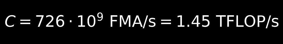
The authors in their paper provide an example FER calculation using multiple chips and architectures. The below equations walk the read through the Alveo U250 design.


In the world of CPUs, higher clock speed (frequency) is almost always synonymous with better performance. On FPGAs, the relationship is more complex and often counter-intuitive. Synthesis tests on the Alveo U250 revealed that as a design utilized a higher percentage of the available compute resources (DSPs), the maximum achievable clock frequency actually decreased.
This might sound like a negative trade-off, but the empirical results prove otherwise. The key finding was that "despite the lower frequency reached, exploiting as much resources as possible pays in terms of performance."
This highlights a fundamental difference in design philosophy. For example, a design using only 20% of the U250's compute resources might achieve a high clock speed of ~325 MHz, but it delivers less than 150 GFLOP/s. In contrast, a design that packs in ~80% of the resources runs at a slower ~240 MHz, yet it delivers a vastly superior throughput of over 400 GFLOP/s. For FPGAs, total throughput—achieved by maximizing parallelism—is far more important than the raw clock speed of any single element.

Conclusion: A New Era for Reconfigurable Computing
FPGAs are rapidly becoming key players in the HPC ecosystem, moving from a complex niche to an accessible and powerful option for accelerating scientific workloads. However, to harness their potential, we must understand that they operate by a different set of rules than conventional CPUs and GPUs. The most surprising takeaways from modern benchmarking paint a clear picture of this new reality: FPGAs are now accessible via high-level languages, their performance must be measured empirically, their on-chip memory allows for uniquely flexible parallel access, and they offer exponential speedups for lower-precision math. As the demand for specialized, energy-efficient computing grows, will trading precision for performance become the new standard for HPC workloads?


Comments